Component evaluation
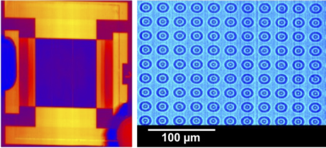
Hyperspectral imaging can also be used in component tests (downstream of the production process). The issues can vary considerably, e.g. OLEDs can be fully spectrally characterized or the printing of microstructures can be monitored. In the case of OLEDs, for example, the active layer can be monitored, while at the same time contacting and other production details are also visible in the HSI. With printed microstructures, the focus is more on the uniformity of the surface. The aim of the inspection must therefore be defined in each case, and the implementation is then carried out using the methods of 'hard modeling' and 'soft modeling' outlined above.

OLED at 1279 nm and printed microstructures at a wvelength of 1397 nm
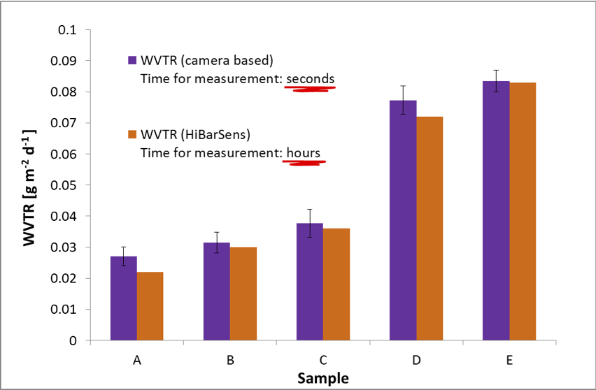
The following describes an application that goes far beyond this. For the encapsulation of OLEDs in particular, so-called high-barrier films are required that have the lowest possible water vapor transmission rate (WVTR). The WVTR is investigated on high-precision measuring devices using laser diode spectroscopy of water vapor in the ppb range (HiBarSens®), although the measurement times can range from days to several weeks due to the diffusion-based WVTR. WVTR is caused by microscopic defects and inhomogeneity of the high-barrier films. These defects ('pinholes') and irregularities are statistically distributed over the surface and should have a spectral effect. Based on the HSI data of the barrier films and a corresponding multivariate and image-processing calibration, the WVTR can be determined within seconds. The monitoring of the actual product property or the entire barrier film thus becomes inline-capable for the first time.

Determination of WVTR rates of HSI against the reference; advantageous are the time constraints for Hyperspectral Vision
